- 您现在的位置:买卖IC网 > Sheet目录17359 > ADR4530BRZ (Analog Devices Inc)IC VREF SERIES PREC 3V 8SOIC
Ultralow Noise, High Accuracy
Voltage References
Data Sheet
FEATURES
ADR4520/ADR4525/ADR4530/ADR4533/ADR4540/ADR4550
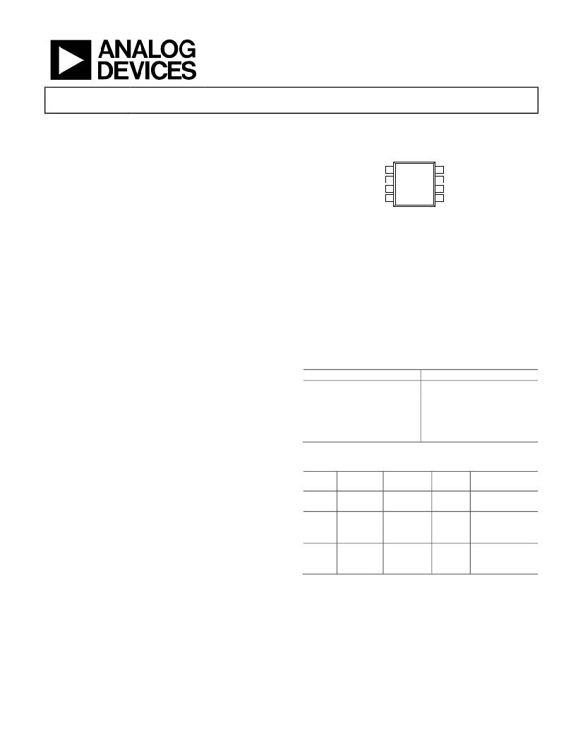
PIN CONFIGURATION
Maximum temperature coefficient (TCV OUT ): 2 ppm/°C
Output noise (0.1 Hz to 10 Hz)
ADR4520/ADR4525/
ADR4530/ADR4533/
ADR4540/ADR4550
Less than 1 μV p-p at V OUT of 2.048 V typical
Initial output voltage error: ±0.02% (maximum)
Input voltage range: 3 V to 15 V
NC 1
V IN 2
NC 3
TOP VIEW
8
7
6
TP
NC
V OUT
Operating temperature: ?40°C to +125°C
Output current: +10 mA source/?10 mA sink
Low quiescent current: 950 μA (maximum)
Low dropout voltage: 300 mV at 2 mA (V OUT ≥ 3 V)
8-lead SOIC package
APPLICATIONS
Precision data acquisition systems
High resolution data converters
High precision measurement devices
Industrial instrumentation
Medical devices
Automotive battery monitoring
GENERAL DESCRIPTION
GND 4 (Not to Scale) 5 NC
NOTES
1. NC = NO CONNECT.
2. TP = TEST PIN. DO NOT CONNECT.
Figure 1. 8-Lead SOIC
The ADR4520/ADR4525/ADR4530/ADR4533/ADR4540/
ADR4550 devices are high precision, low power, low noise
voltage references featuring ±0.02% maximum initial error,
excellent temperature stability, and low output noise.
This family of voltage references uses an innovative core
topology to achieve high accuracy while offering industry-leading
temperature stability and noise performance. The low, thermally
induced output voltage hysteresis and low long-term output
voltage drift of the devices also improve system accuracy over
Table 1. Selection Guide
Model
ADR4520
ADR4525
ADR4530
ADR4533
ADR4540
ADR4550
Output Voltage (V)
2.048
2.5
3.0
3.3
4.096
5.0
time and temperature variations.
Table 2. Voltage Reference Choices from Analog Devices
A maximum operating current of 950 μA and a maximum low
dropout voltage of 300 mV allow the devices to function very
well in portable equipment.
The ADR4520/ADR4525/ADR4530/ADR4533/ADR4540/
ADR4550 series of references is provided in an 8-lead SOIC
package and is available in a wide range of output voltages, all of
which are specified over the extended industrial temperature
range of ?40°C to +125°C.
V OUT (V)
2.048
2.5
5.0
Low Cost/
Low Power
Micropower
Ultralow
Noise
High Voltage,
High Performance
Rev. 0
Information furnished by Analog Devices is believed to be accurate and reliable. However, no
responsibility is assumed by Analog Devices for its use, nor for any infringements of patents or other
rights of third parties that may result from its use. Specifications subject to change without notice. No
license is granted by implication or otherwise under any patent or patent rights of Analog Devices.
Trademarks and registered trademarks are the property of their respective owners.
One Technology Way, P.O. Box 9106, Norwood, MA 02062-9106, U.S.A.
Tel: 781.329.4700 www.analog.com
Fax: 781.461.3113 ?2012 Analog Devices, Inc. All rights reserved.
发布紧急采购,3分钟左右您将得到回复。
相关PDF资料
A9CAA-0602F
FLEX CABLE - AFG06A/AF06/AFE06T
ADR4533BRZ
IC VREF SERIES PREC 3.3V 8SOIC
A9BBA-0203F
FLEX CABLE - AFF02A/AF02/AFF02A
ADR4520BRZ
IC VREF SERIES PREC 2.048V 8SOIC
RBC06DRTI
CONN EDGECARD 12POS DIP .100 SLD
A9BAG-0603F
FLEX CABLE - AFF06G/AF06/AFE06T
MIC2546-1BM
IC SW CURR LIMIT DUAL 16-SOP
ADR430ARZ
IC VREF SERIES PREC 2.048V 8SOIC
相关代理商/技术参数
ADR4530BRZ_PROMO
制造商:Analog Devices 功能描述:IC V REF 15VIN 3V +/-0.02%
ADR4530BRZ-R7
功能描述:IC VREF SERIES PREC 3V 8SOIC RoHS:是 类别:集成电路 (IC) >> PMIC - 电压基准 系列:- 标准包装:2,000 系列:- 基准类型:旁路,可调节,精度 输出电压:1.24 V ~ 16 V 容差:±0.5% 温度系数:- 输入电压:1.24 V ~ 16 V 通道数:1 电流 - 阴极:100µA 电流 - 静态:- 电流 - 输出:20mA 工作温度:-40°C ~ 85°C 安装类型:通孔 封装/外壳:TO-226-3、TO-92-3(TO-226AA)成形引线 供应商设备封装:TO-92-3 包装:带卷 (TR)
ADR4533
制造商:AD 制造商全称:Analog Devices 功能描述:Ultralow Noise, High Accuracy
ADR4533ARZ
功能描述:IC VREF SERIES PREC 3.3V 8SOIC RoHS:是 类别:集成电路 (IC) >> PMIC - 电压基准 系列:- 标准包装:1,000 系列:- 基准类型:旁路,可调节,精度 输出电压:2.495 V ~ 36 V 容差:±0.5% 温度系数:标准值 34ppm/°C 输入电压:2.495 V ~ 36 V 通道数:1 电流 - 阴极:1mA 电流 - 静态:- 电流 - 输出:100mA 工作温度:0°C ~ 70°C 安装类型:表面贴装 封装/外壳:TO-243AA 供应商设备封装:SOT-89-3 包装:带卷 (TR)
ADR4533ARZ_PROMO
制造商:Analog Devices 功能描述:IC V REF 15VIN 3.3V +/-0.0
ADR4533ARZ-R7
功能描述:IC VREF SERIES PREC 3.3V 8SOIC RoHS:是 类别:集成电路 (IC) >> PMIC - 电压基准 系列:- 产品培训模块:Voltage Reference Basics 标准包装:100 系列:- 基准类型:旁路,精度 输出电压:4.096V 容差:±0.075% 温度系数:50ppm/°C 输入电压:- 通道数:1 电流 - 阴极:1µA 电流 - 静态:- 电流 - 输出:10mA 工作温度:0°C ~ 70°C 安装类型:表面贴装 封装/外壳:8-SOIC(0.154",3.90mm 宽) 供应商设备封装:8-SOIC 包装:管件
ADR4533BRZ
功能描述:IC VREF SERIES PREC 3.3V 8SOIC RoHS:是 类别:集成电路 (IC) >> PMIC - 电压基准 系列:- 标准包装:1,000 系列:- 基准类型:旁路,可调节,精度 输出电压:2.495 V ~ 36 V 容差:±0.5% 温度系数:标准值 34ppm/°C 输入电压:2.495 V ~ 36 V 通道数:1 电流 - 阴极:1mA 电流 - 静态:- 电流 - 输出:100mA 工作温度:0°C ~ 70°C 安装类型:表面贴装 封装/外壳:TO-243AA 供应商设备封装:SOT-89-3 包装:带卷 (TR)
ADR4533BRZ_PROMO
制造商:Analog Devices 功能描述:IC V REF 15VIN 3.3V +/-0.0
